 Both IBM and Intel have announced what they are calling major jumps forward in the design of microchips.
They both centre on building transistors using so-called high-k metal gates, which after almost seven years of industry research in the area, it’s claimed will lead to increases in the speed and power of chips for another decade.
The high-k metal gates reduce current leakage and will be used to replace the polysilicon gate electrode currently in use. It does this because the new material holds its charge longer.
It is understood that Intel is further ahead in the process, with the release of computers based on the next chip types by the end of the year. A most fortunate dovetail with Vista being released, which requires a lot of horsepower to run at usable speeds.
Intel said its new family of chips, code-named Penryn, will have 410 million transistors, using the new materials combined with the 45-nanometer technology manufacturing process. This compares with about 280 million in current chips. Intel also said electrical leakage will be reduced by about 30 percent.
Batting off the Intel claims of it being in products this year, Bernie Meyerson, chief technologist for IBM Systems and Technology Group retorted, “It’s almost meaningless to say I’m going to ship a chip first. Yes, you can do that. It doesn’t mean that you are actually going to put it into a server; there is a ton of work to get to that.”
IBM said they will be putting it “out the door in a product in roughly in the 2008 time frame.”
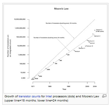
Intel are trotting out Moore’s law again (the number of transistors on an IC doubles every two years), claiming that these advantages will enable it to be maintained. Many people view this as somewhat of a marketing message by Intel, rather than a law.
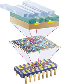
It’s understood that the approach of IBM and Intel differ. Intel are mounting the components on top of the silicon, where IBM are mounting theirs inside the silicon. IBM’s approach potentially gives them the advantage of being able to build many levels on top of each other.
What the heck is a High-K material?
Intel’s view of it is that “High-k” stands for high dielectric constant, a measure of how much charge a material can hold. Example of High-k materials are hafnium dioxide (HfO2), zirconium dioxide (ZrO2) and titanium dioxide (TiO2).